The promises of quantum computation rely on quantum bits (also called qubits) and their ground-breaking potential—yet to this day, they are difficult to produce and manipulate. The most current, advanced designs rely on superconducting circuits with Josephson junction. The production of quantum circuits interconnecting up to ten qubits has been achieved. Although less advanced, qubits using electron spins in silicon are generating significant interest due to the potential for very large-scale integration, combined with Complementary Metal Oxide Semi-conductor, or CMOS technology.
Spintrowhat ?
Spintronics marries electronics and magnetism. While the current electronics is entirely based on the manipulation of the electric charge carried by the electrons, spintronics uses their spin. Electrons have three physical characteristics: their mass, their charge and their spin. For this last intrinsic characteristic, everything happens as if the magnetic moment of the electron was related to the direction of internal rotation of this one around an imaginary fixed axis. For the electrons, the spin can take only two values:
- +1/2 spin said "up"
- or -1/2 spin said "down",
corresponding to the fact that it can only turn in one direction or in the 'other.
This property can be used to obtain new functionalities, for example to code, process or transmit information. A wide variety of innovative devices using electron spin can be realized. These devices combine magnetic materials that serve as a polarizer or spin analyzer and conductive, insulator or semiconductor materials.
A building block for different spin qubits
The MOS-QUITO project aims to develop a functional "building block" produced entirely in CMOS technology on a 300 mm wafer, taking advantage of the state-of-the-art silicon-on-insulator technology available at the 300-mm CMOS platform of CEA-Leti1. This single, yet versatile building block can be tuned to operate in different types of spin qubits. These different qubits will be characterized and benchmarked against key criteria (i.e. fidelity and speed). The project also includes the development of a toolkit of low-temperature peripheral control electronics—low-noise amplifiers, RF generators and multiplexers in particular—based on the same technology.
At the end of 2016, the first step was achieved when the scientists produced a dual-gate field-effect transistor on Silicon On Insulator (SOI) technology, whose conductive channel is made of a silicon nanowire. In the silicon channel, the gate electrodes control two quantum dots confining holes and arranged in series, very close to one another. The first is used to define the qubit, the second, to read it. The qubit can be manipulated simply and efficiently through microwave modulation of the voltage applied to the first gate. It is important to note that this method is possible due to use of the hole transistor rather than electrons: the holes have better spin-orbit coupling, which makes it possible to alter their spin through an oscillation of their position in space.
1 Leti, a technology research institute of the CEA, pioneers micro and nanotechnologies, tailoring differentiating applicative solutions that ensure competitiveness in a wide range of markets. It is one of the CEA’s entity participating in MOS-QUITO project.
2 Inac is a joint CEA-UGA research institute. It is a major actor in fundamental research on condensed matter, soft matter and cryogenics in Grenoble and it is the entity of CEA coordinating the MOS-QUITO project.
"Our unique qubit demonstrator brings CMOS technology closer to quantum spintronics" said Silvano De Franceschi, from CEA (INAC2) and coordinator of project MOS-QUITO "The next step will involve coupling a few qubits and defining how to interconnect more of them.

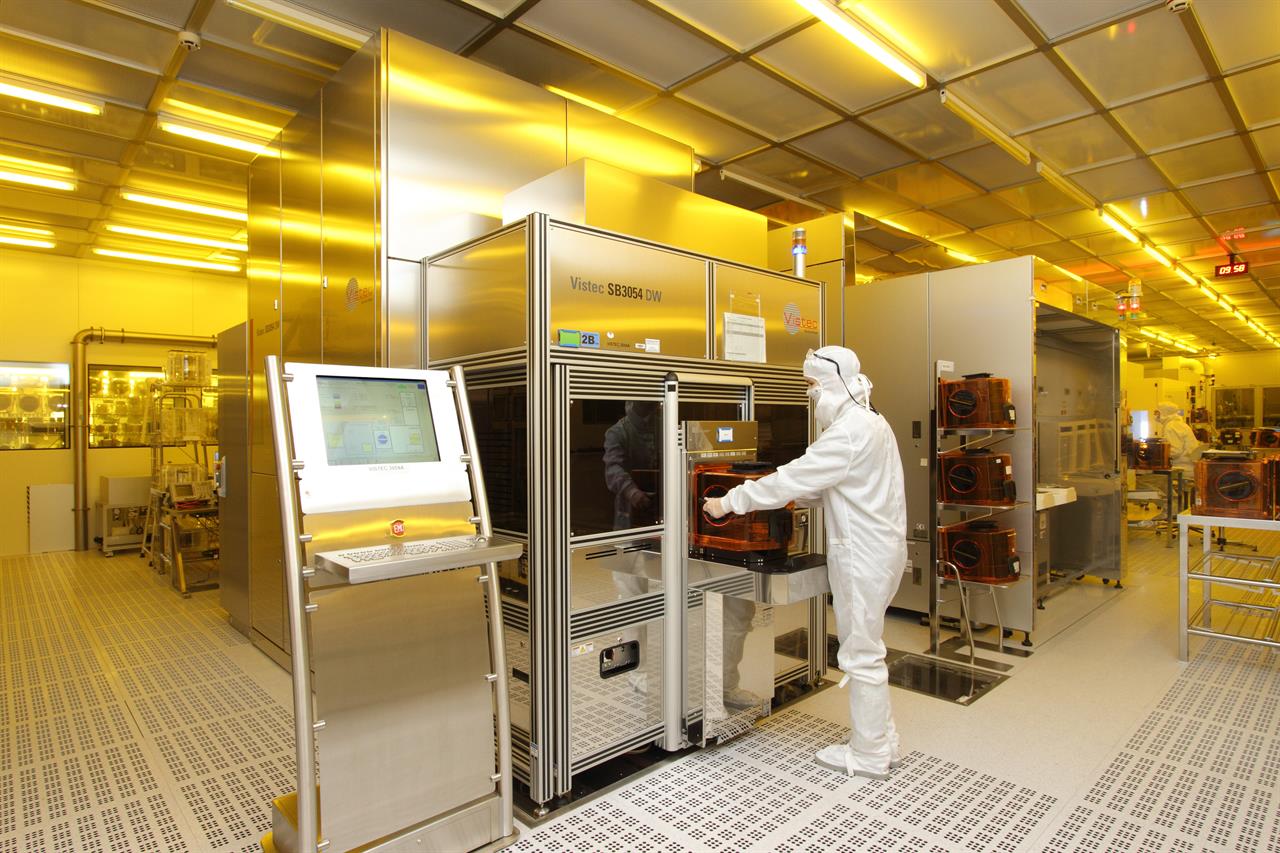
Lithography machine Vistec SB3054, at CEA Leti, used to define dense gates. © Patrick Avavian/CEA
About MOS-QUITO

Coordinated by the CEA, MOS-QUITO brings together, from April 2016 to March 2019, 6 partners from 5 European countries. Granted with 3,5M € of EU funding, the project will have an holistic approach and offer a wider opportunity to harness the tremendous proven capabilities of integrated CMOS technology to become a key driver of quantum technology development.