Intelligent systems based on connected objects are developing rapidly in all sectors, from space to agriculture as well as in all areas of mass consumption. By 2020, nearly 50 billion objects could be on the market. IoT devices require significant autonomy and combine communications, sensors, calculating capacity and memory.
Developed in particular at the CEA1, magnetic random access memory (MRAM) technology is particularly suited to the IoT as it is non-volatile2 and consumes little energy. With this in mind, the aim of the GREAT3 project is to evaluate its potential beyond the memory function.

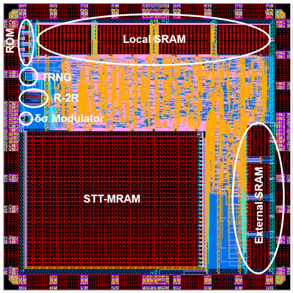
The demonstrator being built by the GREAT consortium. © GREAT
According to Guillaume Prenat, coordinator of the H2020 GREAT project and researcher at CEA-Inac, this technology “can also be used for radiofrequency communications and measurements of magnetic fields.”
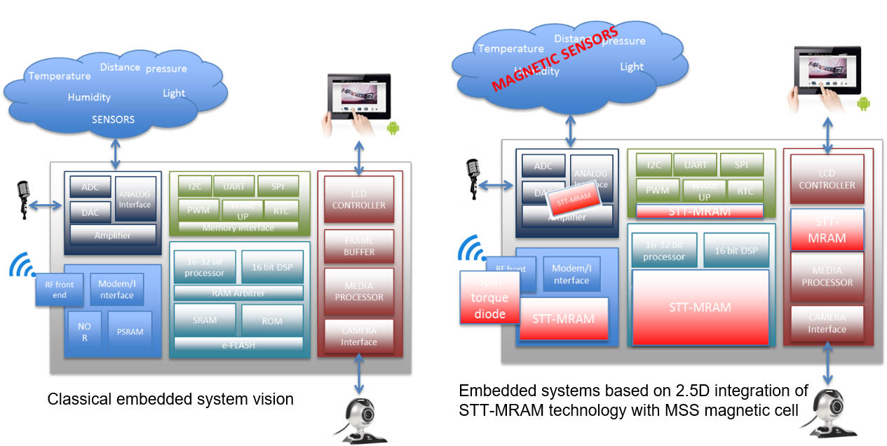
The idea is to integrate the digital and analogue functions (sensors and radiofrequency communications) as well as memories on the same chip.
“By stacking the different layers combining these three functionalities, we greatly simplify manufacturing. We need only one fabrication mask set instead of three, thereby reducing the cost,” explains Prenat.
The CEA team’s first step was to define and produce the individual magnetic components on a single chip. The next step involved designing the integrated circuits and defining a demonstrator, currently in fabrication, with the three targeted functionalities. On the other hand, researchers use numerical simulations to determine the improvement in performance using this technology for various applications proposed by companies of the advisory board.
“We are particularly targeting applications requiring both low energy and relatively high processing capability, for which our technology could be particularly attractive.”
What results can be expected from GREAT?
“We hope to have an operational magnetic CMOS circuit with a performance that correlates well with the simulations. It’s the first time we’ve come this far in building circuits. There’s some real momentum in the field!”

Scheme of the integration of GREAT technology into different functions of a complete electronic system. © GREAT
1 The research was done at the Institute for Nanoscience and Cryogenics (Inac), a joint CEA-UGA research centre in Grenoble specialising in condensed matter, soft matter and cryogenics.
2 A non-volatile memory stores data even if the power is turned off.
3 GREAT stands for heteroGeneous integRated magnetic tEchnology using multifunctional stAndardized sTack.
About GREAT
From January 2016 to December 2018, the GREAT project brings together, under the coordination of CEA, nine partners from three European Union countries and an associate country. With an EU grant of €4.5 million, the project will deliver a test chip with advanced multifunctional standardized stack (MSS) technology along with system-level simulation and design of a representative M2M IoT platform integrating MSS.
