Composite materials made of a stack of two-dimensional (2D) materials have drawn much attention recently thanks to the possibility to control and engineer their band structure by a proper choice of the individual 2D layers. In these composite materials, the interaction at the interface is of van der Waals type owing to the chemical inertness of the adjacent layers, i.e. with no available dangling bonds. As pointed out in earlier studies, the van der Waals coupling is supposed to be weak (few 10 meV) with minor effect on the atomic and electronic structures of the individual layers. However, lattice mismatch or crystal misorientation associated with some orbital overlap can give rise to atomic or electronic fluctuations (such as Moiré patterns) and lead to new physical properties. A deep understanding of van der Waals interactions in such heterostructures is thus pivotal for designing 2D materials-based heterostructures.
In this work, conducted jointly by three laboratories of our institute (Spintec, PHELIQS and MEM), researchers studied the effect of van der Waals interaction on the atomic and electronic structure of the vertical 2D heterostructure MoSe
2/few-layer graphene on SiC. This heterostructure has been fabricated in ultrahigh-vacuum by molecular beam epitaxy, so as to get high quality interfaces. By studying this nearly perfect structure, they have been able to show that the interlayer interaction goes well beyond a weak van der Waals interaction. Firstly, using highly sensitive techniques such as grazing incidence x-ray diffraction at the ESRF (European Synchrotron Radiation Facility), they pointed out an alignment of the MoSe
2 and graphene lattices. No other rotational variants were found, meaning unique epitaxial registry of the heterostructure. Interestingly, by combining spectroscopic data by k-PEEM at ELETTRA (Italian synchrotron radiation facility) and first principles calculations, they demonstrated the existence of a large charge transfer between the MoSe
2 monolayer and graphene sheets, leading to a bandgap opening in the few-layer graphene. A lower bound of the bandgap is estimated to be about 250 meV which is much higher than the previously reported bandgaps in graphene.
Those results show that stacking two-dimensional materials through van der Waals interaction enables to tailor the atomic and electronic properties of individual layers. In particular, it opens a new way to induce a bandgap in few-layer graphene.
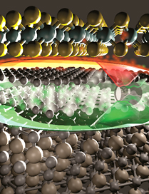
Artistic view of the heterostructure MoSe
2/bi-layer graphene with the band structures calculated by DFT approach showing a large bandgap opening induced by the charge transfer.