Applications of quantum phenomena require low-temperature functioning in order to preserve the essential properties of quantum states. Integrating classical electronics at the same temperature as the quantum device is a challenge in order to control and detect quantum states with greater speed and efficiency while limiting the wiring towards the instrumentation at room temperature. How to develop dedicated cryogenic electronics based on the known technology of CMOS (
Complementary Metal Oxide Semiconductor) components and compatible with silicon quantum bits?
Researchers from IRIG and Leti have prototyped hybrid circuits combining silicon quantum-dot devices with a conventional trans-impedance amplifier (TIA). The TIA is particularly well suited for measuring the current across a semiconductor quantum-dot system (in the pico-ampere range). These nanometer-sized quantum dots have quantized electronic states with an energy spectrum that can be detected as a function of a gate voltage by measuring a current corresponding to single electron transport through the quantum structure.
Trans-impedance amplifiers integrated with current measuring devices are designed and fabricated with the commercial 28 nm fully depleted silicon-on-insulator (FDSOI) CMOS technology at STMicroelectronics. The chip of the nano-device to be measured was placed side by side with the TIA chip or both quantum and conventional systems were realized on the same chip (
Figure). The circuit with the TIA operates at 10 mK with only 1 μW of power consumption, which avoids the heating of the cryostat. It has a linear response up to ±40 nA with a bandwidth of 2.6 kHz. The assembly has a circuit footprint of only 0.1 mm x 0.1 mm. These technical data are very promising for quantum applications at the lowest temperatures. In a more complete version, the chip integrates other analog and digital functions (multiplexer, buffer, signal amplifier, oscillator, level shifter) to make current measurements under excitation in the GHz range.
Following this proof of concept in the realization of a cryogenic TIA, further improvements will focus on increasing the bandwidth of the amplifier for even faster current sensing schemes.
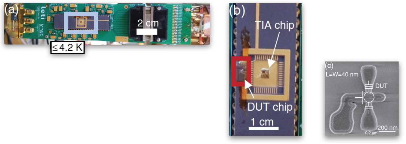
Realization of the TIA with the device to be measured.
a. Circuit board with the connectors,
b. Chip carrier with the TIA; (DUT=quantum dot chip),
c. SEM image of the FDSOI device with source and drain contacts and quantum dot formed under the gate (circle).
Loïc Le Guevel is a PhD student supervised by Gaël Pillonnet (CEA-Leti) and Louis Jansen (IRIG’s Pheliqs laboratory). He is a member of the Grenoble Silicium Quantique research group headed by Maud Vinet.