Silicon photonics has many advantages for data communication, signal processing and optical detection applications. The main one lies in the fact that it is based on materials compatible with CMOS technologies used in the manufacture of electronic chips, such as silicon (Si) or germanium (Ge). However, the remaining challenge is to design components that are capable of generating optical signals while integrated on a silicon chip, all of which must operate at room temperature.
For several years, researchers at IRIG have been looking at ways to make one of the group IV materials compatible with microelectronics light-emitting. A major step towards this goal has been taken with the development of a laser source made of a germanium-tin alloy (GeSn). Indeed, starting at a proportion of 6 to 8% of tin, this GeSn alloy has an atomic structure, known as "
direct gap", which allows the emission of light. However, the incorporation of tin into germanium does not occur naturally and, furthermore, the laser regime has been limited to cryogenic temperatures to date. Continuous experimental efforts have been made since the early 2010s to increase the Sn concentration in GeSn alloys. For example, since the first demonstration of lasing at 90 K in 2015, the maximum operating temperature has been steadily improved from 180 K to 270 K by increasing the Sn concentration from 16 to 20%. By 2018, researchers at IRIG had achieved mid-infrared lasing at a temperature of 230 K. The following year, they succeeded in obtaining laser emission over a very wide frequency range and at an operating temperature of up to 273 K, just a few steps below room temperature.
In collaboration with CEA-LETI and the Centre de nanosciences et de nanotechnologies (C2N) in Paris-Saclay, researchers at IRIG have designed an optimized GeSn cavity in the shape of a micro-disk (
Figure). Thanks to this structure, they have just carried out the experimental demonstration of a laser regime at room temperature with this device. This was made possible thanks to an alloy (Ge
0.83Sn
0.17) richer in tin than those previously used and to a better heat dissipation in the stack of the layers. This heat dissipation was made possible by using a better adapted pedestal architecture including the use of layer-by-layer hybridization techniques.
The highest temperature of the laser regime is now 32°C, for an emission wavelength in the mid-infrared range of 3.5 µm. This result is a major breakthrough as it shows the potential of this CMOS-compatible alloy for future digital applications (information processing) or nano-optical sensors.
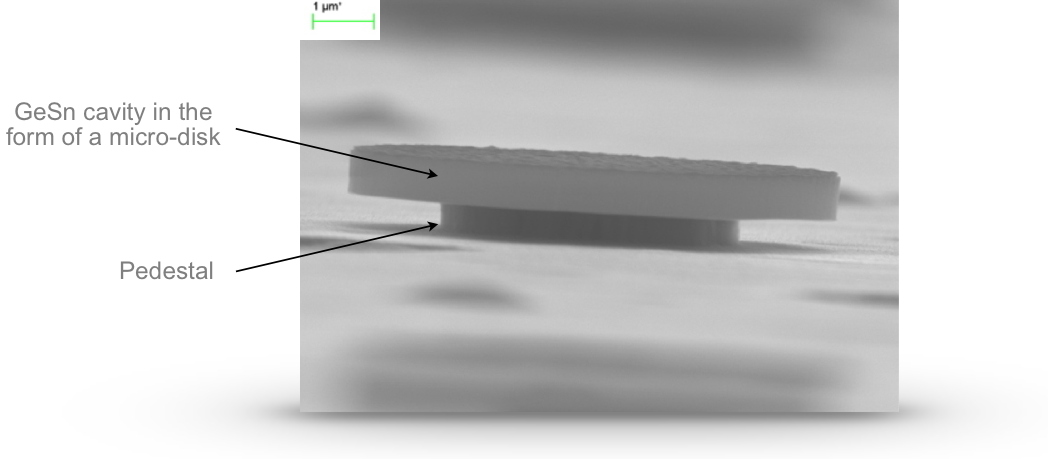
GeSn laser micro-disk with a diameter of 8 µm on an aluminum nitride pedestal. Credit CEA
In semiconductor physics, the “gap” or the band gap, is the energy interval between the lowest energy state of the conduction band and the highest energy state of the valence band. We speak of direct gap when these two extremums correspond to the same quasi-momentum (momentum associated with the wave vector in the first Brillouin zone), and indirect gap when the difference between the wave vectors of these two extremums is non-zero.