The development of semiconductor nanostructures has been achieved through a good control of their fabrication, for instance by Molecular Beam Epitaxy (MBE). For a long time, this technique has been limited to the growth of planar structures such as quantum wells, inducing a spatial confinement of charge carriers in the perpendicular direction. New challenges, such as the realization of single-photon emitters for quantum communications, require a stronger confinement in two or three directions, obtained by making nanowires and quantum dots.
The growth of nanowires is usually seeded by a liquid droplet of a few nanometers, which determines the diameter of the nanowire. During the growth, quantum dots can be inserted by changing abruptly the composition of the molecular beam. This “Vapor-Liquid-Solid” mechanism combines a vapor phase in the beam, a liquid phase in the droplet, and a solid phase in the nanowire. At the seed-nanowire interface, the growth was supposed to take place through the nucleation of a one-monolayer step and its propagation along this interface. For years, this was a mere assumption. The Nanomax setup at Centre for Nanoscience and Nanotechnology (C2N) Palaiseau, France, now allows to observe this process
in-situ in a modified electron microscope.
Researchers at IRIG and at Neel Institute (Nano Physic and Semiconductors NPSC, Grenoble), are interested in II-VI semiconductors combining a metal (Zn or Cd column II of the Mendeleev table) and a chalcogen (Se or Te column VI). These materials are particularly interesting as active optical elements, for light emission or photovoltaics. II-VI nanowires can be grown with a gold seed which is solid and crystalline instead of liquid: this is the “Vapor-Solid-Solid” growth, which is expected to provide sharper interfaces when inserting a quantum dot.
Observing the growth of ZnTe nanowires at Nanomax revealed two original aspects: the role of the lattice mismatch at the nanowire-seed interface, and a self-regulation of the step dynamics.
Gold and ZnTe crystals feature the same lattice, but the ZnTe unit cell is 3/2 larger than that of gold. When the gold monolayer located at the interface is progressively replaced by a ZnTe monolayer, a strong mismatch strain appears at the step, which creates a barrier against the formation of such step.
Alternatively, a different step configuration, made of 2 ZnTe monolayers facing 3 gold monolayers, shows practically no mismatch making this configuration more favorable. And indeed, the Nanomax investigation revealed this growth proceeds for liquid nanoparticles (Fig. 1 and movie 1). And when nanoparticle is liquid the propagation is made both with one or two monolayers steps (Movie 2).
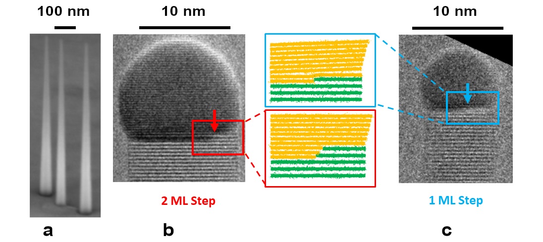
Figure: (a) ZnTe nanowires grown in MBE cluster; (b) Nanomax image showing the gold seed at the top of the ZnTe nanowire, with a two-monolayer step at the interface; the step (indicated by the arrow) propagates from right to left; (c) idem, with a one-monolayer step. The schemes in-between display the Au atomic planes (in yellow) and the ZnTe planes (in green) for the two configurations. Credit CEA