Detection in the Short-Wave Infrared (SWIR: 1.5–3.0 µm) is critical to many applications, such as imaging under low-visibility conditions (e.g., fog), gas detection, and biomedical diagnostics. Currently, the most sensitive SWIR detectors rely on
direct bandgap* III-V and II-VI semiconductors*. In addition to their complex and costly fabrication—often requiring cryogenic cooling—these devices are grown via
epitaxy* on specific substrates, which complicates their integration with
CMOS silicon technologies*. These limitations are driving the development of alternative materials, such as the recently stabilized group IV semiconductor alloys of the germanium-tin (Ge₁₋ₓSnₓ) family, which can be epitaxially grown onto silicon wafers. These materials exhibit a direct bandgap at wavelengths longer than 2 µm and tin contents
x greater than 8%, which enables high optical absorption.
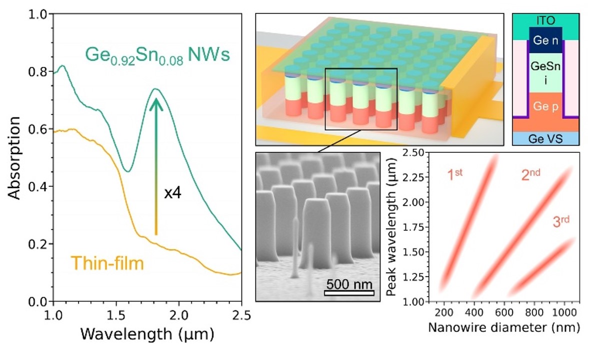
The researchers nanostructured thin films of Ge0.92Sn0.08 by etching them into ordered arrays of vertical nanowires, each with diameters of a few hundred nanometers and heights of one micrometer. This architecture enhances the electromagnetic field within the semiconductor structures by trapping light through
leaky-mode resonances (LMRs)*. As a result, light absorption is quadrupled compared to a conventional thin film. By adjusting the nanowire diameter from 200 to 1 000 nm, the resonance peaks can be precisely tuned for wavelengths between 1 and 2.4 µm. Each nanowire then functions like an infrared-optimized nano solar cell: at a resonant wavelength determined by its dimensions, the nanowire network efficiently converts the incident flux of light energy into an electrical current that can be directly read by a measurement instrument. The device operates without an external voltage and thus at a reduced power consumption.
© CEA-Irig/PHELIQS
Figure : Schematic of a GeSn nanowire array photodetector exhibiting enhanced infrared absorption and an LMR peak that is tunable with the nanowire diameter.
Working at room temperature and with a precise control of its spectral absorption, this device paves the way for a new generation of compact infrared sensors that can be directly integrated into
eye-safe LiDAR systems* and infrared spectrometers. Ongoing work aims at improving their sensitivity by optimizing the fabrication process, particularly through better surface treatment to reduce electronic defects that cause signal loss. Additionally, efforts are focused on extending their operation into the mid-wave infrared (MWIR: 3–8 µm) by increasing the tin concentration in the GeSn alloy. At longer term, improvements in GeSn epitaxy processes will enable higher tin content, reaching the long-wave infrared (LWIR: 8–20 µm) and thus enabling the development of multispectral imaging systems across the entire infrared range.
III-V and II-VI semiconductors*: crystalline materials composed of elements from the III and V, or II and VI columns of the periodic table, such as GaAs or HgCdTe, widely used in optoelectronics. Their electronic structure generally features a direct bandgap*, which depends on their composition. This enables targeting of different operating wavelengths.
Bandgap*: In a semiconductor crystal, energy range where no electronic states are allowed. It is bounded by the extrema of the valence and conduction bands. The emergence of a bandgap enables the control of populations of free electrons or free holes and allows for optical transitions, forming the foundation of modern electronics and optoelectronics.
Epitaxy*: it is the science of crystal growth on a substrate. During this process, deposited atoms arrange according to the lattice structure of the underlying crystal, enabling the production of high-quality materials. III-V semiconductors must be deposited on specific III-V substrates (e.g., GaAs, InP), which increases fabrication costs and limits their integration with CMOS technologies on silicon*.
CMOS technology on silicon*: CMOS stands for Complementary Metal-Oxide-Semiconductor, an industrial process used to manufacture electronic circuits on silicon wafers. This technology enables large-scale, reliable, and cost-effective production.
Leaky-mode resonances (LMRs)*: Depending on the wavelength and the nanowire's dimensions, particular light path channels resulting in temporarily trapped light that propagates through the nanowire before escaping.
LiDAR systems*: LiDAR stands for Light Detection And Ranging. These remote sensing systems determine the distance between a sensor and an object by measuring the travel time of a laser pulse reflected by the object.
-
UMR : Univ. Grenoble Alpes (UGA), CEA, Grenoble INP UGA - IRIG/PHELIQS.
-
Fundings : ANR (SINPHONI), CEA PTC (SAGE), UGA (SAGE).
-
Collaborations : CEA LETI (Laboratoire d'électronique et des technologies de l'information).