The photovoltaic industry is fast becoming one of the major sources of energy, the most widely deployed on the planet today. Further reducing its environmental impact is now a competitiveness driver for the industry, as well as an essential innovation axis to maintain the sector's growth rate and better meet societal challenges.
Committed to this approach for several years, the CEA at INES has set itself the challenge of developing a photovoltaic panel employing heterojunction technology (HJT) by seeking to combine everything that one would expect of a "premium" product with:
- Exemplary power and reliability characteristics,
- A significantly reduced environmental impact,
- Components manufactured in Europe.
To lead our teams in their technological choices, a Life Cycle Assessment sensitivity study was carried out. This allowed focusing on the most critical aspects of the carbon footprint: the silicon wafers, the glass front panel and the aluminum frame.
- The reduction of the carbon footprint on a cell scale is possible by using Norwegian-made silicon wafers with a thickness of 130 microns instead of 170µm, based on poly-silicon of German origin.
- The cells, made in France on the CEA's pilot line at INES, include innovations that limit the consumption of indium and silver, critical metals, during the optimization of the metallization and interconnection processes
- The panel, with a glass-back sheet configuration adapted for the residential sector, is assembled in France within the dedicated technological platform of CEA at INES and uses a thinner glass (2mm). A frame made of plant material (wood species, available in Europe) replaces its aluminum frame.
- A "design for recycle" approach has led to the choice of fluorine-free thermoplastic encapsulants and back sheets of European origin, which will facilitate recycling.
To guarantee high efficiency, which is also a critical lever, the interconnection of the cells by a paving (or gapless) process has been favored. This eliminates the gap between the solar cells and interconnects them by creating a 1 mm overlap between cells while keeping the interconnection strips. It densifies the panel and increases its power per sqm (or conversion efficiency).
The demonstration module shows a power of 566 Wp and embeds heterojunction technology cells with an average efficiency of 22.9%. It achieves a very low carbon footprint of 317 kgCO2eq/kWp compared to standard Chinese products (700 to 800 kgCO2eq/kW) and places our laboratories among the leaders in Europe.
This result is mainly due to
- The electricity mix of the places where the main components are manufactured: Germany, Norway and France. These countries have a low carbon mix estimated at 650 gCO2eq/kWh, 29 gCO2eq/kWh and 52 gCO2eq/kWh respectively, compared to the Chinese mix with a carbon balance of 1023 gCO2eq/kWh.
- The thickness of the glass and the silicon wafers also contribute to a significant reduction in the carbon footprint.
- The replacement of the aluminum frame by a frame made of vegetable material (wood) has reduced the carbon footprint by more than 50 kgCO2eq/kWp
Details of the eco-design approach used
The reduction of the environmental impact considers more than 15 criteria to evaluate a photovoltaic panel, of which the carbon footprint is currently the reference criterion by the industry and public authorities.
The Life Cycle Assessment was carried out in accordance with ISO14040 and ISO14044 standards. The scope of the study was limited to the module manufacturing phase (from cradle to door). The various parameters of the module were taken into account (number of cells, wafer thickness, power, etc.). The functional unit was "1 kWp of a photovoltaic module". The production location of the different components of the value chain was taken into account.
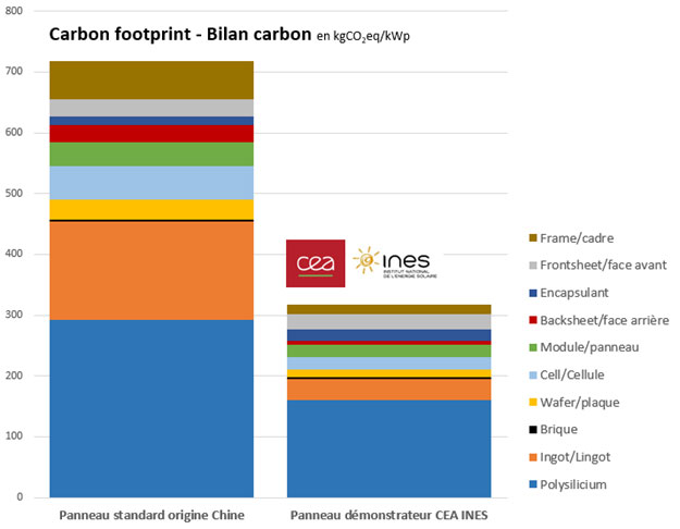
Comparative life cycle analyses of a standard panel manufactured in China and the demonstrator panel made by CEA at INES
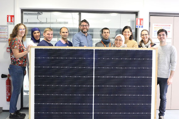
Eco-designed demonstrator panel, 317 kg CO2 eq/kWp, 566 W power, made by the CEA teams at INES © CEA