KEY FIGURES
€140 million in investment
17,000 sq. m of facilities including 2,000 sq. m of clean rooms
Chambéry
| The materials unit
with silicon ingot growth, slicing, and characterization capabilities. The platform has lab-scale (60 kg) and industrial-scale (1,200 kg) pilot lines and industrial-grade equipment for cutting ingots into bricks and slicing them into wafers.
The cell unit
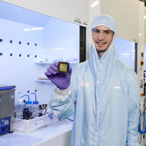
for perovskite silicon tandem technology conversion efficiency, cost, and process scaleup. CEA-Liten has been obtaining excellent performance on its industrial-scale silicon process equipment, helping to make heterojunction technology more competitive since 2005. The platform's current target is to achieve yields of at least 25% on silicon and, ultimately, exceed 30% on perovskite silicon tandem cells, a technology that is rapidly gaining traction at the CEA and other research organizations worldwide. The main technological hurdles are perovskite materials' stability, homogeneous deposition on large (greater than 100 cm2) surfaces, and processes compatible with industrial-scale production. The cell unit is home to some of the platform's flagship facilities: - A 1,300 sq. m ISO 8 clean room with advanced perovskite material production equipment. The Solar Photovoltaic Platform can manufacture and optimize PV cells on a variety of silicon substrates, and can conduct earlier-stage R&D on highly innovative perovskite silicon tandem cells.
- The HET fablab is representative of an industrial heterojunction cell production line, soon to scale up to M10/M12 wafers (up to 210 mm x 210 mm). This high-speed line (2,400 cells per hour) is used to complete the necessary proof-of-concept testing on new cell technologies, ensuring optimal transfer to our manufacturing partners and, ultimately, the rollout of new technologies in France and across Europe.
|
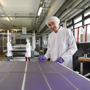
The PV module and system unit
designs high-performance PV modules and systems, with a particular focus on heterojunction and tandem cells. The unit uses eco-innovation methods to develop process bricks and novel integrated PV solutions. Finally, the unit couples PV modules with systems that collect and convert the energy produced into electricity and that enable safe, efficient management.
The PV module and system unit develops processes and materials for the packaging of heterojunction and tandem cells in high-performance photovoltaic modules. The unit possesses extensive know-how not only in development, but also in modeling and predicting performance. It also develops innovative integrated, recyclable, eco-designed PV concepts. The unit couples PV modules with systems that collect and convert the energy produced into electricity and that enable safe, efficient management.
|
|