 Function
Researcher
Experimental physicist. Nanomagnetism and spintronics
Current interest

Spin transport and spin currents in lateral nanodevices
Spin to charge interconversion using spin Hall and Rashba effects, topological insulators
Spin transfer torque and domain wall depinning
Magnonics
Magnetic tunnel junctions and MRAMs
Resume

Since November 2007,
permanent researcher at CEA-Grenoble, Nanostructure and Magnetism Lab & Spintec
October 2007-September 2006,
Professor Assistant, University of Tokyo, Institute for Solid State Physics, Prof. Y. Otani
June 2004-July 2006,
Post-Doctoral fellowship (
CNRS, France), Laboratoire de Photonique et de Nanostructures, Dr. G. Faini
March 2000-June 2004,
PhD in Material Science, Université catholique de Louvain (Belgium) and Université Paris Sud Orsay (France),
Unité de Physico-Chimie et Physique des Matériaux (Belgium), Pr. L. Piraux and Unité Mixte CNRS/Thalès (France), Pr. A. Barthelemy.
•
Transport électronique dans des nanofils magnétiques connectés par voie lithographique
•
Electronic transport in magnetic nanowires connected by lithography.
1999-2000,
DEA Sciences des Matériaux (DEA in Materials science), Université Paris-Sud Orsay (France), option Thin Films.
April-September 1999,
Michigan State University (U.S.A.), Pr. W. Pratt and Pr. J. Bass
Experimental skills
Magneto-transport measurements down to ultra low temperatures and very high magnetic field (down to 20 mK and up to 7T).
Electron beam lithography using e-beam nanowriters: JEOL 5DIIU and LEICA EBPG 5000+
Thin films growth by D.C. sputtering, Molecular Beam Epitaxy. Electrodeposition in confined media. Metal evaporation by joule effect or e-gun. Transfer method: lift-off, ion beam etching and reactive ion etching. Nano-object manipulation.
AFM/MFM, Ferromagnetic resonance, SEM, Auger and X-ray spectroscopies, Squid/AGFM Magnetometry, XRD.
Micromagnetic simulations using Oommf software
Why going to nano?

The
ebeam lithography can combine top/down and bottom/up approaches to further reduce the dimension of our devices. We take advantage of the new dominant physical mechanisms to elaborate novel materials with extended functionalities. Starting either from thin films and heterostructures or from smaller building blocks (nanoparticles, nanowires), we can fabricate different devices and measurements environnements.
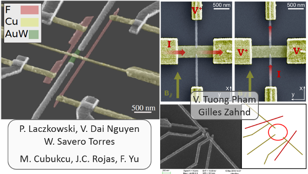
Nanowires are model objects in such concern. They are the basic electrical circuitry. Their physical properties are governed by the interplay between their dimension and the typical length scales of magnetism and electronic transport. Magnetization reversal, magneto-transport, action of magnetization on the current but also action of the current on the magnetization are some examples of the novel properties existing
at the bottom.
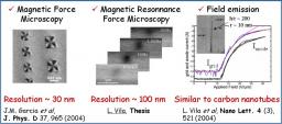
Moreover nanowires offer new opportunities in nanotechnologies. They are not only the subject of basic research but also novel tolls for the characterization of nano-objects. They can also be integrated in systems taking advantages of their reduced dimension and high aspect ratio. For instance they are efficient field gradient sources in magnetic force and magnetic resonance force microscopies, and efficient field emission electronic sources.
Selected Articles (full list can be found here):
Highly efficient and tunable spin-to-charge conversion through Rashba coupling at oxide interfaces
E Lesne, Y Fu, S Oyarzun, JC Rojas-Sánchez, DC Vaz, H Naganuma, ...
Nature Materials (2016)
Spin to Charge Conversion at Room Temperature by Spin Pumping into a New Type of Topological Insulator: α-Sn Films
JC Rojas-Sánchez, S Oyarzún, Y Fu, A Marty, C Vergnaud, S Gambarelli, ...
Physical Review Letters 116 (9), 096602 (2016)
Spin Pumping and Inverse Spin Hall Effect in Platinum: The Essential Role of Spin-Memory Loss at Metallic Interfaces
JC Rojas-Sánchez, N Reyren, P Laczkowski, W Savero, JP Attané, ...
Physical Review Letters 112 (10), 106602 (2014)
Spin-to-charge conversion using Rashba coupling at the interface between non-magnetic materials
JCR Sánchez, L Vila, G Desfonds, S Gambarelli, JP Attané, JM De Teresa, ...
Nature Communications 4 (2013)
Non-adiabatic spin-torques in narrow magnetic domain walls
C Burrowes, AP Mihai, D Ravelosona, JV Kim, C Chappert, L Vila, A Marty, ...
Nature Physics 6 (1), 17-21 (2010)
Evolution of the spin Hall effect in Pt nanowires: size and temperature effects
L Vila, T Kimura, YC Otani
Physical Review Letters 99 (22), 226604 (2007)