NANOCHARACTERIZATION PLATFORM
Characterization of advanced materials and components supporting disruptive innovation
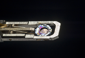
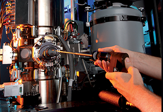
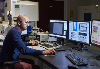
The nano-characterization platform offers an access to over 100 researchers that operate state-of-the-art equipment and analyse properties of innovative materials and components.
With more than 50 world-class equipment, researchers supports companies of all sizes, from startups to major groups. They provide in-depth analysis, investigating new materials and components properties — morphological, physical, chemical, and electrical behaviors. They also collaborate with nanocharacterization tools suppliers to improve their equipment performance.
To be more specific, our researchers characterize advanced materials, complex stacks, new devices and manufacturing processes using customized analysis and characterization protocols. They also leverage large scale infrastructures, partnering with ESRF and ILL, as well as other key academic partners.
They also provide results and interpretations, such as atomic-scale 2D mapping, multi-scale 3D reconstructions, multi-scale composition analysis (from μm down to sub-nm), crystallographic structures, optical properties, and surface compositions.
|
What expertise do industrial partners receive?
• Nanocharacterization techniques and protocols
• Advanced sample preparation
• Algorithms for processing experimental data
• Eco-friendly materials and technologies
|
|
Cutting edge preindustrial equipment
• Aberration corrected analytical transmission electron microscopy: Titan Ultimate by ThermoFisher Scientific
• 3D morphology using small-angle X-ray scattering: Xeuss 2 by Xenocs
• Tandem time of flight mass spectrometer: nanoTOF by Physical Electronics
• High energy photoelectrons spectrometer for buried interfaces: Quantes by Physical Electronics
• FlexTAP atom probe tomography by Cameca
|
|
How to work with the nano-characterization platform?
CEA-Leti’s teams support the innovation needs of industrial partners throughout all development stages via bilateral contracts and shared laboratories. The platform works with more than a dozen partners, such as: SERMA Technologies, Physical Electronics (ULVAC-PHI) and Attolight.
|