Finding alternatives to PZT’s thermal and environmental challenges
PZT (lead zirconate titanate) has a high crystallization temperature, usually between 500 °C and 700 °C. This makes developing transparent piezoelectric thin film stacks particularly challenging. Not only can growing PZT on glass damage the substrate, it can also compromise the performance of other materials in the stack. Another issue is the lead in PZT, which has been in the crosshairs of the EU directive on the restriction of hazardous substances in electrical and electronic equipment (RoHS) for fifteen years now. Lead-free alternatives are urgently needed as exemptions for specific uses must be periodically renewed, putting the electronics supply chain under increased pressure.
KNN, a lead-free material for integrated piezoelectric microactuators
The advance toward a lead-free alternative to PZT involved first depositing and then integrating KNN (potassium-sodium niobate) films on 200 mm silicon wafers. The high-quality KNN films, 1.9 microns thick, were sputter deposited onto 200 mm SOI by Sumitomo Chemical of Japan and integrated into various actuator devices by CEA-Leti using industry-compatible MEMS processes. The devices performed nearly as well as their lead-containing counterparts. This achievement marks a significant step towards replacing PZT in piezoMEMS and, specifically, in microactuators.
Process innovations enable transparency for PZT and its potential successors
A wafer-to-wafer piezoelectric layer transfer process developed by CEA-Leti resolves the thermal budget issues associated with the material, making it possible to integrate PZT capacitors into various layer stacks or substrates for both actuator and sensor applications. Here, piezoMEMS devices were fabricated using both deposited and layer-transferred PZT films on 200 mm silicon wafers. There was no significant difference in performance between the deposited and transferred films. Looking ahead, PZT films or other piezoelectric materials, such as KNN, could be integrated onto CMOS and glass substrates, or onto any stack that cannot tolerate PZT crystallization temperatures.
A clear path to ITO/PZT/ITO capacitors on glass
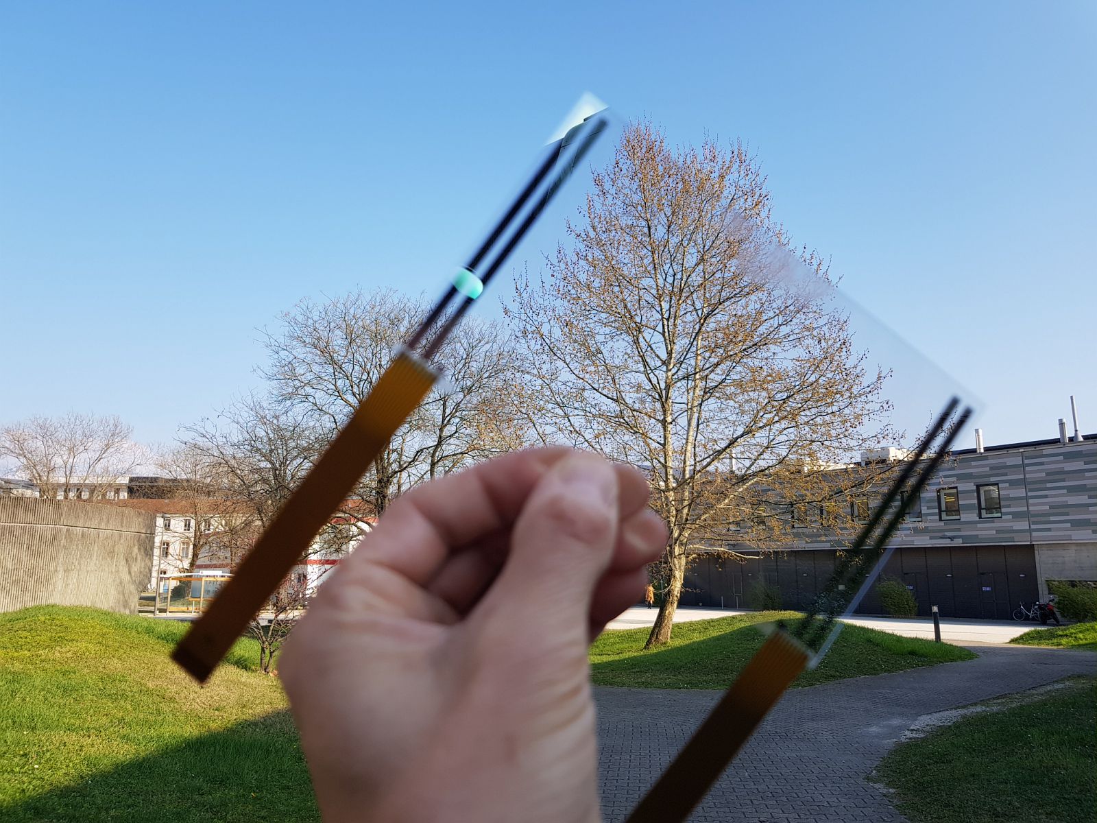
CEA-Leti’s new wafer-to-wafer transfer process was also used to make fully integrated transparent ITO/PZT/ITO capacitors on glass, bypassing not only the thermal budget issues of PZT crystallization, but also the negative impacts on ITO electrical and optical performance. The transparent piezoelectric stacks were made by growing PZT films on platinized silicon wafers and bonding them to glass wafers, enabling the integration of PZT stacks into capacitor devices using MEMS processes. The devices exhibit an average transparency of approximately 80%—in some cases, up to 94%—and demonstrate a transverse piezoelectric coefficient suitable for actuation purposes. In this research, a vibrating glass plate (3.12 cm X 3.12 cm) using a PZT capacitor (35.9 mm²) performed on par with models

Piezoelectric actuators integrated on glass surface
These advances were presented at Transducers 2023 in Kyoto, Japan in June 2023 and at Eurosensors XXXV in Lecce, Italy in September 2023.