MICROSYSTEMS 200 MM AND 300 MM PLATFORM
A world-class R&D facility
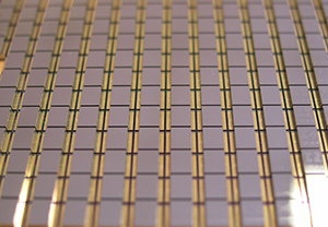
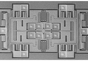
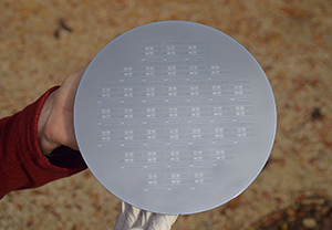
The Microsystems 200 mm and 300 mm platform develops sensors, actuators, RF microsystems (MEMS-RF) and integrated packaging solutions.
The platform's highlyqualified staff, equipment, and international activities make it the world's leading center for high performance microsystems R&D.
The objectives of the R&D conducted at the platform are to optimize the actual sensors and actuators, their integration, their reliability while reducing component cost and energy consumption to transfer them to industrial partners. The platform investigates also new materials in particular new piezoelectric material generations, creates, and develops new components with the associated technological channels.
The microsystems platform targets the mobile phone, medical, automotive, industry, aeronautics, spatial and defense markets.
The platform has 20 ongoing strategic partnerships with components and systems manufacturers and end users. Its activities cover the entire component-development chain, from simulation, design, and technology development to demonstrator systems and industrial scale-up. Other activities include advanced morphological and electrical characterization and reliability studies.
|
What expertise do industrial partners receive?
• Design and simulation of microsystems components • Development of new manufacturing processes
• Manufacturing and scale-up of new technological channels
• Electromechanical, acoustic, thermal tests and microcomponents reliability
• Transfer to industrial founders
|
|
Cutting edge preindustrial equipment
• Multiphysics simulation tools (COMSOL, ANSYS, CADENCE, SPICE...)
• Specific equipment for MEMS manufacturing: DRIE, vapor HF, vacuum bonder, stepper with dual-side alignment...
• Access to the nano-characterization platform of Leti (more than 50 world-class equipment)
Characterization and test tools:
• Manual, semi-automated and automated probe systems in controlled environment (temperature and vacuum)
• Material characterization equipment (nano-indenter, traction-compression and micro-traction)
• Mechanical tests (positioning and rate table, vibration shaker)
• Residual gas analysis by spectrometry
• Resistance and reliability tests (climatic chamber, swing board)
• Microscope (infrared, thermography, digital holographic microscope)
• Laser vibrometer
• Climatic chamber
• Anechoic chamber
|
|
How to work with
the microsystem platform?
CEA-Leti's teams support the needs of its industrial partners (major groups, small and medium-sized companies, and startups) across all or some stages of development, using bilateral contractors or collaborative projects. The platform hosts about twenty industrial partners from mobile phone medical, automotive, industry, aeronautics, special and defense markets.
|