MEMS Reliability
Wafer-level electrical characterization and analysis are essential to improve MEMS performance
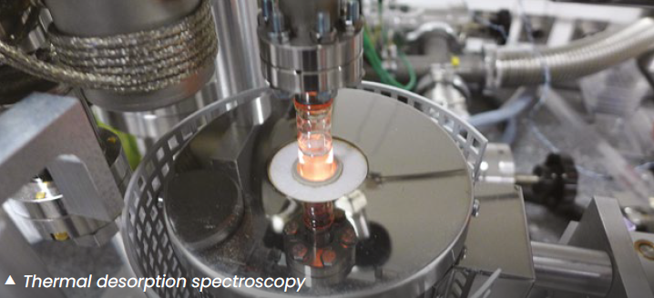
CEA-Leti is home to 70 wafer-level testing probers stations, both automated and semi-automated, for electrical behavior and reliability studies across temperature from -40 °C to 1,000 °C, and down to 2 Kelvin. Some probers also operate under vacuum pressures as low as 10-5 mbar. Complete RGA-TDS (residual gas analysis-thermal desorption spectroscopy) allows outgassing and sorption getter characterization under wafer-level packaging conditions, providing quantitative and qualitative data. This information, combined with CEA-Leti’s modeling and analysis capabilities, helps to improve chip functionality, performance and reliability.
What it can do
CEA-Leti’s wafer-level characterization capabilities allow device developers and manufacturers to understand what is happening inside MEMS devices: - Hermeticity of wafer level sealed cavities,
- Integrated vacuum lifetime,
- Quality factor and resonance frequencies of resonator modes,
- MEMS behavior studies in harsh environmental conditions,
- Deep defects analysis.
|
What makes it unique
CEA-Leti's unique range of wafer-level characterization equipment is backed by a team of experts and by characterization protocols developed at CEA-Leti to extract useful information about the physical phenomena involved in the components behavior. In addition to testing at much wider range of temperatures than standard wafer prober capabilities, CEA-Leti is also home to laser vibrometers, infrared microscopy and lock-in thermography, and the ability to measure and analyze residual gases under vacuum inside volumes as small as 1 mm3. CEA-Leti has also developed specific modelling capabilities that are particularly useful to improving device reliability. Finally, CEA-Leti has access to the CEA Nanocharacterization Platform for additional measurements, such as device morphology.
|
Working with CEA-Leti
CEA-Leti’s wafer-level characterization capabilities are of interest to foundries and fabless companies seeking new insights into the electrical behavior and reliability of their MEMS components. Companies that partner with CEA-Leti gain access to a world-class slate of wafer-level probers and other advanced characterization equipment, all backed by CEA-Leti’s modelling and analysis expertise, plus access to a wider range of measurements like those available at the CEA Nanocharacterization Platform.
Scientific publications
- Duchemin, H., Bouchu, D. (2025). “Sorption getter characterization under wafer-level packaging (WLP) conditions.” Microelectronics Reliability, Volume 168, 2025, 115677
- Boutonnet, C., et al. (2025). “Characterization of a Multi-Channel CMUT Gas Sensor.” Journal of Microelectromechanical Systems, vol. 34, no. 1, pp. 4-14, Feb. 2025
|