
Starting date : Mar. 2019 > Mar. 2024 Lifetime: 60 months
Program in support :

Status of project : in progress

TEAM  Dr.
François Andrieu is the head of Laboratory “Nano-devices for Memory and Computing” at
CEA-Leti, Grenoble, France. He received the M.Sc and Ph.D. degrees from the
Grenoble INP, France in 2001 and 2005, respectively. He has been strongly
involved in the development of the Fully-Depleted-Silicon-On-Insulator (FDSOI)
CMOS technology at Leti and with STMicroelectronics, where he was assigned between
2012-2015 in process-integration and technology-to-design groups. His fields of
interest are: advanced CMOS transistors, stacked nanowires, 3D and
3D-sequential integration, RF CMOS, Silicon spin Qbits, NVM Resistive-RAM and
In-Memory-Computing. He is currently serving as the 2020/2021 Technical Program
Committee Chair of the European Solid-State Device Research Conference
(ESSDERC), as well as a TPC member of the IEDM, VLSI-TSA and SSDM conferences.
He is the author or co-author of more than 14 patents, 200 conference abstracts
or refereed journal. To contact :François Andrieu Dr.
François Andrieu is the head of Laboratory “Nano-devices for Memory and Computing” at
CEA-Leti, Grenoble, France. He received the M.Sc and Ph.D. degrees from the
Grenoble INP, France in 2001 and 2005, respectively. He has been strongly
involved in the development of the Fully-Depleted-Silicon-On-Insulator (FDSOI)
CMOS technology at Leti and with STMicroelectronics, where he was assigned between
2012-2015 in process-integration and technology-to-design groups. His fields of
interest are: advanced CMOS transistors, stacked nanowires, 3D and
3D-sequential integration, RF CMOS, Silicon spin Qbits, NVM Resistive-RAM and
In-Memory-Computing. He is currently serving as the 2020/2021 Technical Program
Committee Chair of the European Solid-State Device Research Conference
(ESSDERC), as well as a TPC member of the IEDM, VLSI-TSA and SSDM conferences.
He is the author or co-author of more than 14 patents, 200 conference abstracts
or refereed journal. To contact :François Andrieu

Project Coordinator: CEA-Leti
Partners: N/A
Investment: € 2.7 mi
EC Contribution: € 2.7 mi

Releases- D. Bosch et al., "Comparative experimental study of junctionless and inversion-mode nanowire transistors for analog applications," in 2020 International Symposium on VLSI Technology, Systems and Applications (VLSI-TSA), Hsinchu, Taiwan, Aug. 2020, pp. 126–127, doi: 10.1109/VLSI-TSA48913.2020.9203690. https://ieeexplore.ieee.org/document/9203690
- Bosch et al., "All-operation-regime characterization and modeling of drain current variability in junctionless and inversion-mode FDSOI transistors," presented at the Symposium of VLSI Tech, 2020.
https://ieeexplore.ieee.org/document/9265036 - M.
Ezzadeen et al., “Ultrahigh-Density 3-D Vertical RRAM With Stacked Junctionless Nanowires
for In-Memory-Computing Applications ,”
IEEE Trans. Electron Devices, pp. 15,2020, doi:10.1109/TED.2020.3020779. https://ieeexplore.ieee.org/document/9199382
- Barraud et al, "3D RRAMs with Gate-All-Around Stacked Nanosheet Transistors for In-Memory-Computing," presented at the IEEE IEDM conf., 2020.
|
| Stakes
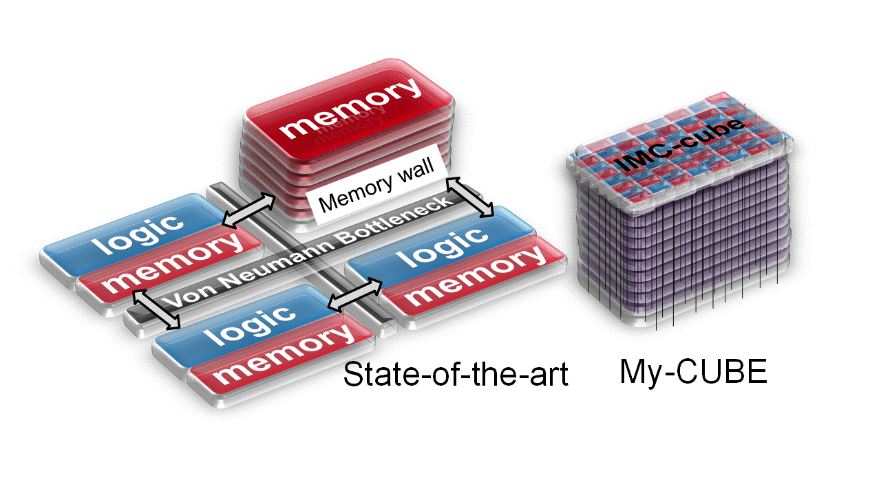
The project aims are: - To demonstrate scalability of In-Memory-Computing and fabricate an IMC-cube
- To develop multi-level 3D-monolithic integration of logic/memory devices at 450°C
- To couple energy-efficient junctionless nanowire and vertically resistive RAM devices
- To design an IMC-cube and exploit its full potential.
OBJECTIVES
- Historical scaling of Complementary-Metal-Oxide-Semiconductor (CMOS) devices is no longer a cornerstone of integrated circuits capable of leveraging the future “data deluge” from the Cloud and cyber-physical systems. At system level, computing performance is now strongly power-limited and the majority of this power budget is used by data transfers between logic and memory circuit blocks in widespread Von-Neumann design architectures. An emerging computing paradigm solution that overcomes this “memory wall” involves processing the information in situ through In-Memory-Computing (IMC).
- Today’s memory technologies are ineffective for In-Memory-Computing, which will process billions of data items just like the human brain. Things may change with the emergence of three key enabling technologies: non-volatile resistive memory, new energy-efficient nanowire transistors and 3D-monolithic. My-CUBE will leverage these technologies to produce a functionality-enhanced system involving close entangling of logic and memorization. Only this type of technology is capable of supporting the IMC concept’s scalability.
- Based on a holistic approach from system to material, My-CUBE’s unique solution relies on a new class of nanotechnology, combining at fine-grain level the high capacity of non-volatile resistive memory with new junctionless nanowire transistors, 3D-interconnected at low-temperature, to perform data-centric computations. A 3D IMC accelerator circuit will be designed, manufactured and measured. This targets a 20x reduction in (Energy x Delay) Product vs.Von-Neumann systems.
IMPACT
- MYCUBE takes advantage of Europe’s current momentum in technology/ circuit innovative solutions. This project proposes differentiating nano- technology to the benefit of the semiconductor industry, fabless circuit design companies and academics.
- CEA-Leti will ensure design and fabrication as a direct add-on for existing CMOSs to be fully optimized for the new IMC computing paradigm. This technology, which adds smartness to memory/storage, is not only suitable for data-abundant applications but, more broadly, is the kernel of ultimate low-power, energy-efficient integrated circuits in Europe.
RECENT RESULTS
- Today, storage-class memories like high-density 3D crossbar Resistive-Random-Access-Memories (RRAM) are promising for applications requiring a large amount of on-chip memory. RRAM is a leading candidate due to its high density, good scalability, low operating voltage, and easy integration with CMOS devices. Another attractive aspect of RRAM is their ability to perform primitive Boolean logic operations for in-memory and neuromorphic computing. However, if the classical one transistor / one RRAM (1T1R) design is the most reliable architecture for in-memory-computing (IMC), the cell size remains limited by the conventional access transistor.
- Within the frame of My-CUBE project, we have explored a novel 3D 1T1R memory cube. This 1T1R architecture benefits from the high density of vertically stacked Nanosheet transistors, developed for advanced CMOS, which feature excellent scalability and 3D integration scalability [1]. This novel 1T1R 3D RRAM architecture is competitive from the crossbar density point of view, while getting rid of any sneak path current, enabling large-scale in-memory-computing. Some of the RRAM-based architectures for IMC proposed in the literature imply programming operations. Here, we promote the "scouting logic" approach, which is only based on reading operation, ensuring high memory endurance [2].
- More precisely, the technical results we demonstrated are the following:
- The architecture we propose integrates HfO2-based OxRAM with select junctionless transistors based on low-voltage Gate-All-Around (GAA) stacked Nanosheet technology. A bitcell size of 23.9×F2/N is achieved ('N' being the number of stacked-Nanosheet) as well as a very high write and read parallelism. Extensive characterization of junctionless transistors and OxRAMs has been performed to show their ability to be co-integrated inside a same 1T1R memory cell [3].
- Electrical characterization of 4kbits OxRAM arrays shows a large memory window (HRS/LRS=20) up to 104 cycles with a current compliance of 150µA, compatible with the performances of our junctionless transistors.
- Then, we experimentally demonstrate scouting logic operations capability with 2 operands, which should be extended to 4 operands thanks to an original two cells/bit "double coding" scheme assessed by SPICE simulation. Finally, we evidenced that this computing scheme is 2 times more energy efficient than a write-verify approach.
- This results show how promising this technology is for in-memory-computing and more widely for energy-efficient computing circuits.
|