EVENT
Discover CEA-Leti's latest results in plasma etching, cleaning and emerging semiconductor manufacturing technologies showcased.
The workshop gathers scientists, engineers and industry partners to discuss advances and challenges in dry etching, plasma processing and related technologies for semiconductor, MEMS and emerging applications.
DISCOVER CEA-LETI’S MAJOR SCIENTIFIC RESULTSWith 5 papers, (one keynote) the institute will present this year’s major scientific results at PESM 26. including the following topics:
-
Advanced photonics platforms based on SOI, SiN, and heterogeneous integration
-
GeTe plasma etch process development for RF switch applications
-
HBr/H+ Plasma Etching of GeSe-GeTe Chalcogenide Films for Integrated Photonics: Morphology of Blanket and Patterned Structures
-
Reactive ion etching of LiNbO3 waveguides: Influence of fluorine-based gas chemistry on morphology and etch rates
-
Investigating F Plasmas for Chamber Cleaning Efficiency and Environmental Sustainability in Microelectronics
CEA-Leti scientific papers
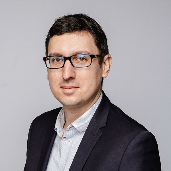
DON'T MISS KARIM HASSAN TALK ON ADVANCED PHOTONICS PLATFORMS BASED ON SOI, SIN, AND HETEROGENEOUS INTEGRATION
Session 2: Plasma etching processes for more than Moore applications
June 08, 1:00 - 1:30 p.m
Advanced photonics platforms based on SOI, SiN, and heterogeneous integration
Karim
HASSAN
Lab Director LIPS (Silicon Photonic Integration Laboratory)
© UtopikPhoto - CEA
ABOUT PLASMA ETCH AND STRIP PROCESSES FOR MICRO-, NANO- AND BIO-TECHNOLOGIES
The workshop gathers scientists, engineers and industry partners to discuss advances and challenges in dry etching, plasma processing and related technologies for semiconductor, MEMS and emerging applications.
 More information on PESM’s website