Remaining challenges: Qubit Wiring - Cryogenic Electronics
Published on 12 April 2021
Body text 1
Remaining challenges: Qubit Wiring - Cryogenic Electronics
Back to main menu
Body text 2
what is needed to create a quantum computer?
| First, quantum dots need to be defined and filled with one electron. Electrostatic gates, similar to those in classical transistors, can be used to define quantum dots. At cryogenic temperature, the individual electrons (or electron holes) held in them can be controlled using the tunnel effect. Application of an external constant magnetic field creates the two-level system.
Then, single and two-qubit operations need to be performed. Single-qubit manipulation is then obtained, for example, by applying a small microwave magnetic field. Each of the numerous qubits experiencing this microwave magnetic field can be made sensitive or insensitive thanks to a local applied electric field that changes the qubit resonance frequency (Stark effect). Two-qubit operations are realized by varying the interaction between two adjacent quantum dots. To switch the interaction on and off, researchers can detune the gates used for the quantum dots or add an additional interaction gate (or exchange gate) between the two dots.
Finally, the state of the qubit needs to be measured, in the so-called readout operation. Readout results from a spin qubit come from a spin-to-charge conversion, which is obtained by coupling the qubit with an additional quantum dot or single-electron transistor (SET). The spin of the qubit can be probed by detection of the change of charge or capacitance. The spacing between the silicon-spin qubits produced in CEA-Leti laboratories is typically 100nm. These dimensions can be reached thanks to immersion lithography. After some 70 years of work on transistor scaling in pursuit of Moore’s Law advances in processing power, we have extensive ability to produce millions of identical objects with high yield and low variability. This is seen as a key asset in the effort to define, operate and read qubits in a reliable and repeatable manner. However, even this is not enough to make quantum computing a reality. Leveraging this remarkable opportunity will require several other critical challenges to be addressed: Qbit Wiring, Cryogenic Electronics, Cryogenic Integration, System-Level Low-Temperature Design.
| 
(c) CEA
|
Qubit Wiring
- To perform universal computation with qubits, it’s necessary to have individual control of each and every qubit within an array of qubits. Such arrays of qubits are conceptually analogous to arrays of pixels, like those in CCD sensors or memory arrays. Thus, any practical quantum computing model could take advantage of existing know-how for addressing pixels within an array to control qubits on a large scale.
The ERC project team has developed a complete architecture that leverages 3D sequential integration and takes into consideration all the technological and physical constraints, and uses two layers of silicon to perform all the quantum operations.  Known as Qucube, it is structured to implement a scalable spin qubit architecture in silicon and to perform large-scale quantum operations with electron spin qubits.
Another QSG effort recently published results aimed at improving quantum dot control and addressability, through the use of embedded detectors and an array of eight MOS quantum dots. The researchers evaluated two methods, a single-lead charge detector and a reprogrammable single-electron transistor. They found great promise for the ability to build a device with a large number of quantum dots, with the two methods offering the
ability to perform real-time measurement of a single charge-tunneling event, which could be used to load single electrons in the structure or read out spin states.
It’s also necessary to find ways to perform basic operations in parallel. The whole point of applying many more qubits to a task is to increase algorithmic efficiency; it’s imperative that the scale-up to hundreds or thousands of qubits does not increase the execution time. One promising line of work by a CEA-Leti group is pursuing the ability to read out a full line of qubits in parallel using RF.
Cryogenic Electronics
- Many of the basic challenges of quantum computing are intertwined. The need for operation at cryogenic temperatures, for example, affects all approaches to quantum technology, not just silicon spin, and all approaches will also require electronics for qubit control and read-out, and interfacing with classical computing systems. This highlights the broad importance of exploring and developing low-temperature CMOS technologies, especially advanced technologies such as FD-SOI, which has the unique property of being able to change its threshold voltage (Vth) and recenter it as a function of the temperature.
In this context, it’s worth noting that one advantage of silicon qubits is that they are robust enough to operate at higher temperatures than superconducting qubits. Experiments have shown that 1K is a reasonable target for silicon-spin operations, with promising early results on fidelity and coherence time — critical factors in creating reliable and robust computing systems. Operation in the 1K range, rather than the mK range (closer to absolute zero), would simplify many of the practical challenges of system operation as it enables larger power to be dissipated.
In addition, developers will need to find ways of effectively linking room-temperature instruments and systems with low-temperature systems without creating information bottlenecks on the inputs and outputs. While work on this is still in progress, it seems likely that it will not be possible to address each qubit "in the refrigerator" from a room
temperature controller and that it will be necessary to develop router-type schemes of directing and multiplexing data. Again, the analogy with memory or CCD arrays in appliable; this is the source of the crossbar-addressing solution. While it reduces the need for wiring, it also requires extremely precise electrostatic control capabilities ideally located as close as possible to the qubit die.
Body text 3

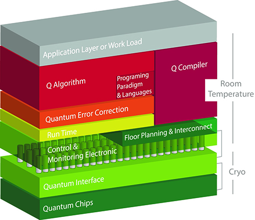
3D ARCHITECTURE, CRYOGENIC LARGE
SCALE COMPATIBLE ARCHITECTURE
Spin qubit architecture in Si to perform large scale quantum operations with electron spin qubits.
FD-SOI AND QUANTUMThe operation of circuits at cryogenic temperatures (<100K) is necessary in a wide range of applications such as infrared sensors, spatial applications, and cryobiology. More recently, CEA-Leti’s researchers have been investigating their use in quantum computing, for reading and controlling quantum bits.
CEA-Leti has published findings on the performance and variability of 28nm CMOS FD-SOI technology for cryogenic applications, down to 100mK. This has provided some of the first experimental measurements and analysis of these circuits at cryogenic temperatures, including study of the drain current and transconductance of FD-SOI transistors, matching, self-heating, and low-frequency noise at temperatures <20K.
|
|
Top page