Testing Silicon Pic
Testing thousands of pic dies in one day
CEA-Leti offers on-wafer photonic integrated circuit (PIC) testing services, including optical, electrical and/or electro-optical tests. Thousands of dies can be measured in one day, depending on circuit complexity and characteristics.
To reach this number, CEA-Leti leverages five automatic probers compatible with 300 mm wafers, and one prober compatible with 200 mm wafers. Only wafer loading is manual. Wafer alignment and measurement are fully automatic.
Optical signal injection
The optical signal—1.3 μm and 1.55 μm telecom wavelengths—is injected through optical fibers and integrated grating couplers with a very precise positioning between each other. An electrical signal is injected through current probes, and a very high frequency signal is injected into co-designed probes and devices to be tested -device design taking into account probe design and vice versa.
Dedicated testing benches
Fully packaged PICs can also be tested on dedicated testing benches. Analog testing can be DC, low/high frequency, and RF up to 67 GHz. Numeric testing can be performed up to 64 Gbs in NRZ and 128 Gbauds in PAM4 modulation technology.
A unique expertise combined with world-class facilities
CEA-Leti’s highly versatile facilities and team of experts help industrials save both time and money, and enjoy access to complex statistics—on or between wafers. The institute’s differentiators include:
- A large choice of measured parameters on-wafer—long before packaging—from passive-circuit optical-injection losses with multiple input/output to DC and high-frequency RF system testing.
- A large choice of functions and circuits to be tested, including waveguides, gratings, lasers, modulators, photodetectors and complex circuits.
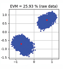 Phase shift keying constellation
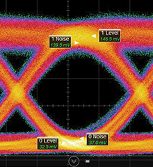 Eye diagram @12,5 Gb/s