ADVANCED PACKAGING
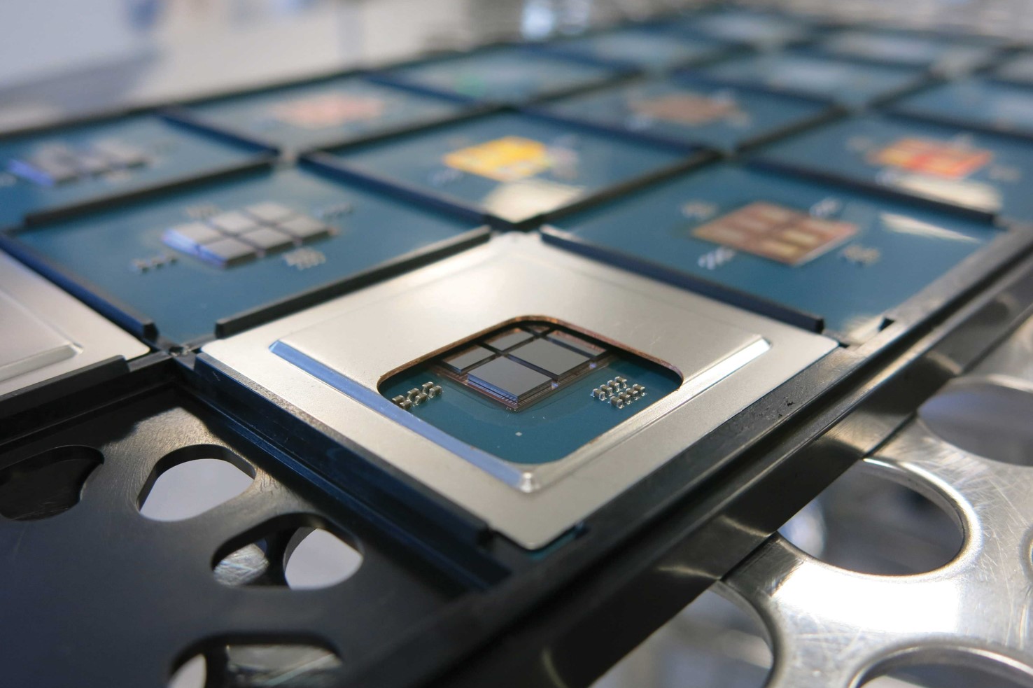
ManuFacturers in a wide range of industries can speed up the development of new products with a “one to many” approach that re-uses Lego-like modules. CEA possesses all the technologies needed to break up monolithic circuits into smaller, modular units called chiplets and reassemble, or “package” them into high-performance, low power 3D integrated circuits for specific use cases and families of chips that offer different levels of performance at different price points, from entry-level to high-end.
CEA’s roadmaps for its chiplet and 3D integration technologies are totally aligned. This means that R&D partners can access innovative modular chiplet architectures and the processes to package the chiplets into 3D integrated circuits or families of circuits to meet a variety of needs without having to develop a specific complex circuit for each use case or implementation scenario. It is possible to pick and choose the features you need to reach the perfect tradeoff between criteria like data transfer rate and power consumption, for example.
Solutions for a wide range of industries
Die-to-wafer hybrid bonding is a 3D integration technique of interest to display and imager makers looking to pack in more pixels and manufactures of processors for high-performance computing looking to boost data transfer rates while keeping power consumption low. In addition to advanced hybrid bonding, CEA offers a large toolbox of solutions such as through silicon vias, bumps, balls, copper pillars, redistribution layers and fan-out wafer-level packaging.
Car manufacturers are always on the lookout for fast, cost-effective ways to add new functions to a variety of vehicle types. CEA offers a baseline chiplet architecture that can be modified to meet specific for a chip or family of chips with a range of functionalities, from multimedia entertainment to advanced driver assistance systems.
Heterogeneous integration is ideal for IoT sensing and signal processing circuits built on separate sensing,
processing, and memory components. CEA has a wide range of design and interconnection options available and can recommend the right combination for your specifications. Circuit-to-circuit optical communication, which depends on the heterogeneous integration of photonic interposers and waveguides, will be the future of
high-performance computing and sensing technologies like LiDAR.
| ![]()
|
|
Chiplets for simpler, faster, cheaper design
|
3D integration for more functions & greater performance |
|
• Simpler design and development for faster, more cost-effective design and development • Lower manufacturing costs due to smaller circuits with higher yields • Greater flexibility to re-use modules for a range of chips within the same product family
|
• Different types of circuits (top-die & bottom-die) can be hybridbonded enabling more interconnects and smaller pixel pitches • Top-die circuits can be connected to the substrate using TSVs to connect the power supply, for example • Heterogenous bonding techniques allow different substrates to be combined
|
CEA’s complete chiplet and 3D integration toolkit from design to integration can rapidly take you from concept to prototype
| “Chiplets and 3D integration offer a one-to-many approach that lets manufacturers develop new products faster and more costeffectively than with monolithic circuits.” |
| 
Aurélie Beaumont, Project Manager, 3D integration, CEA
|